ISO 25498
(Main)Microbeam analysis — Analytical electron microscopy — Selected area electron diffraction analysis using a transmission electron microscope
Microbeam analysis — Analytical electron microscopy — Selected area electron diffraction analysis using a transmission electron microscope
ISO 25498:2018 specifies the method of selected area electron diffraction (SAED) analysis using a transmission electron microscope (TEM) to analyse thin crystalline specimens. This document applies to test areas of micrometres and sub-micrometres in size. The minimum diameter of the selected area in a specimen which can be analysed by this method is restricted by the spherical aberration coefficient of the objective lens of the microscope and approaches several hundred nanometres for a modern TEM. When the size of an analysed specimen area is smaller than that restriction, this document can also be used for the analysis procedure. But, because of the effect of spherical aberration, some of the diffraction information in the pattern can be generated from outside of the area defined by the selected area aperture. In such cases, the use of microdiffraction (nano-beam diffraction) or convergent beam electron diffraction, where available, might be preferred. ISO 25498:2018 is applicable to the acquisition of SAED patterns from crystalline specimens, indexing the patterns and calibration of the diffraction constant.
Analyse par microfaisceaux — Microscopie électronique analytique — Analyse par diffraction par sélection d'aire au moyen d'un microscope électronique en transmission
General Information
Relations
Buy Standard
Standards Content (Sample)
FINAL DRAFT
International
Standard
ISO/FDIS 25498
ISO/TC 202/SC 3
Microbeam analysis — Analytical
Secretariat: JISC
electron microscopy — Selected
Voting begins on:
area electron diffraction analysis
2025-01-31
using a transmission electron
Voting terminates on:
microscope
2025-03-28
Analyse par microfaisceaux — Microscopie électronique
analytique — Analyse par diffraction par sélection d'aire au
moyen d'un microscope électronique en transmission
RECIPIENTS OF THIS DRAFT ARE INVITED TO SUBMIT,
WITH THEIR COMMENTS, NOTIFICATION OF ANY
RELEVANT PATENT RIGHTS OF WHICH THEY ARE AWARE
AND TO PROVIDE SUPPOR TING DOCUMENTATION.
IN ADDITION TO THEIR EVALUATION AS
BEING ACCEPTABLE FOR INDUSTRIAL, TECHNO
LOGICAL, COMMERCIAL AND USER PURPOSES, DRAFT
INTERNATIONAL STANDARDS MAY ON OCCASION HAVE
TO BE CONSIDERED IN THE LIGHT OF THEIR POTENTIAL
TO BECOME STAN DARDS TO WHICH REFERENCE MAY BE
MADE IN NATIONAL REGULATIONS.
Reference number
ISO/FDIS 25498:2025(en) © ISO 2025
FINAL DRAFT
ISO/FDIS 25498:2025(en)
International
Standard
ISO/FDIS 25498
ISO/TC 202/SC 3
Microbeam analysis — Analytical
Secretariat: JISC
electron microscopy — Selected
Voting begins on:
area electron diffraction analysis
using a transmission electron
Voting terminates on:
microscope
Analyse par microfaisceaux — Microscopie électronique
analytique — Analyse par diffraction par sélection d'aire au
moyen d'un microscope électronique en transmission
RECIPIENTS OF THIS DRAFT ARE INVITED TO SUBMIT,
WITH THEIR COMMENTS, NOTIFICATION OF ANY
RELEVANT PATENT RIGHTS OF WHICH THEY ARE AWARE
AND TO PROVIDE SUPPOR TING DOCUMENTATION.
© ISO 2025
IN ADDITION TO THEIR EVALUATION AS
All rights reserved. Unless otherwise specified, or required in the context of its implementation, no part of this publication may
BEING ACCEPTABLE FOR INDUSTRIAL, TECHNO
LOGICAL, COMMERCIAL AND USER PURPOSES, DRAFT
be reproduced or utilized otherwise in any form or by any means, electronic or mechanical, including photocopying, or posting on
INTERNATIONAL STANDARDS MAY ON OCCASION HAVE
the internet or an intranet, without prior written permission. Permission can be requested from either ISO at the address below
TO BE CONSIDERED IN THE LIGHT OF THEIR POTENTIAL
or ISO’s member body in the country of the requester.
TO BECOME STAN DARDS TO WHICH REFERENCE MAY BE
MADE IN NATIONAL REGULATIONS.
ISO copyright office
CP 401 • Ch. de Blandonnet 8
CH-1214 Vernier, Geneva
Phone: +41 22 749 01 11
Email: copyright@iso.org
Website: www.iso.org
Published in Switzerland Reference number
ISO/FDIS 25498:2025(en) © ISO 2025
ii
ISO/FDIS 25498:2025(en)
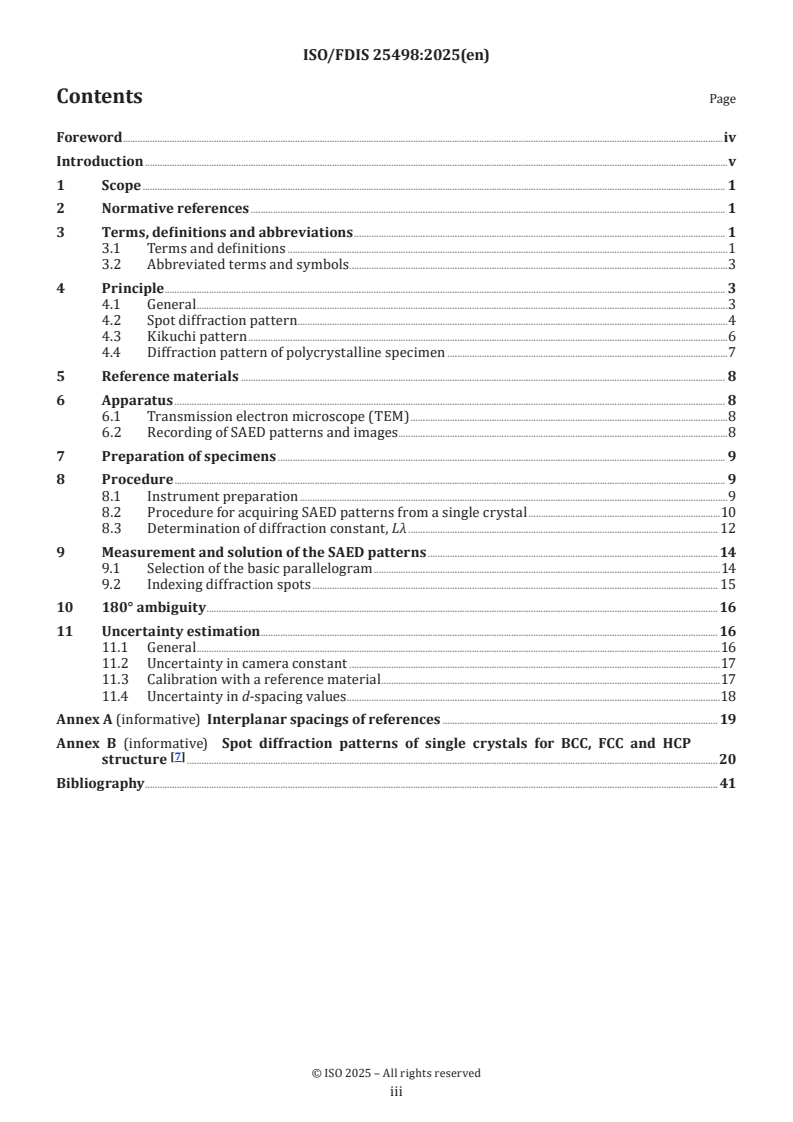
Contents Page
Foreword .iv
Introduction .v
1 Scope . 1
2 Normative references . 1
3 Terms, definitions and abbreviations . 1
3.1 Terms and definitions .1
3.2 Abbreviated terms and symbols.3
4 Principle . 3
4.1 General .3
4.2 Spot diffraction pattern.4
4.3 Kikuchi pattern .6
4.4 Diffraction pattern of polycrystalline specimen .7
5 Reference materials . 8
6 Apparatus . 8
6.1 Transmission electron microscope (TEM) .8
6.2 Recording of SAED patterns and images .8
7 Preparation of specimens . 9
8 Procedure . 9
8.1 Instrument preparation .9
8.2 Procedure for acquiring SAED patterns from a single crystal .10
8.3 Determination of diffraction constant, Lλ . 12
9 Measurement and solution of the SAED patterns . 14
9.1 Selection of the basic parallelogram .14
9.2 Indexing diffraction spots . 15
10 180° ambiguity .16
11 Uncertainty estimation . 16
11.1 General .16
11.2 Uncertainty in camera constant .17
11.3 Calibration with a reference material .17
11.4 Uncertainty in d-spacing values . .18
Annex A (informative) Interplanar spacings of references . 19
Annex B (informative) Spot diffraction patterns of single crystals for BCC, FCC and HCP
[7]
structure .20
Bibliography . 41
iii
ISO/FDIS 25498:2025(en)
Foreword
ISO (the International Organization for Standardization) is a worldwide federation of national standards
bodies (ISO member bodies). The work of preparing International Standards is normally carried out through
ISO technical committees. Each member body interested in a subject for which a technical committee
has been established has the right to be represented on that committee. International organizations,
governmental and non-governmental, in liaison with ISO, also take part in the work. ISO collaborates closely
with the International Electrotechnical Commission (IEC) on all matters of electrotechnical standardization.
The procedures used to develop this document and those intended for its further maintenance are described
in the ISO/IEC Directives, Part 1. In particular, the different approval criteria needed for the different types
of ISO document should be noted. This document was drafted in accordance with the editorial rules of the
ISO/IEC Directives, Part 2 (see www.iso.org/directives).
ISO draws attention to the possibility that the implementation of this document may involve the use of (a)
patent(s). ISO takes no position concerning the evidence, validity or applicability of any claimed patent
rights in respect thereof. As of the date of publication of this document, ISO had not received notice of (a)
patent(s) which may be required to implement this document. However, implementers are cautioned that
this may not represent the latest information, which may be obtained from the patent database available at
www.iso.org/patents. ISO shall not be held responsible for identifying any or all such patent rights.
Any trade name used in this document is information given for the convenience of users and does not
constitute an endorsement.
For an explanation of the voluntary nature of standards, the meaning of ISO specific terms and expressions
related to conformity assessment, as well as information about ISO's adherence to the World Trade
Organization (WTO) principles in the Technical Barriers to Trade (TBT), see www.iso.org/iso/foreword.html.
This document was prepared by Technical Committee ISO/TC 202, Microbeam, Subcommittee SC 3, Analytical
electron microscopy.
This third edition cancels and replaces the second edition (ISO 25498:2018), which has been technically
revised.
The main changes are as follows:
— Scope has been revised;
— ISO/IEC 17025 has been moved from normative references to bibliography;
— Figure 1 has been replaced;
— Subclause 6.3 has been deleted;
— Subclause 8.3.6 has been deleted, the content of 8.3.6 has been moved to 8.3.2;
— Subclause 9.2.5 has been added and the following subclause has been renumbered;
— Clause 11 has been revised, 11.1,11.2,11.3 and 11.4 have been added;
— Subclauses B.4.1 and B.4.2 have been added;
— Bibliography has been updated and ISO/IEC Guide 98-3 (GUM:1995) has been added.
Any feedback or questions on this document should be directed to the user’s national standards body. A
complete listing of these bodies can be found at www.iso.org/members.html.
iv
ISO/FDIS 25498:2025(en)
Introduction
Electron diffraction techniques are widely used in transmission electron microscopy (TEM) studies.
Applications include phase identification, determination of the crystallographic lattice type and lattice
parameters, crystal orientation and the orientation relationship between two phases, phase transformations,
habit planes and defects, twins and interfaces, as well as studies of preferred crystal orientations (texture).
While several complementary techniques have been developed, for example microdiffraction, nano-
diffraction, convergent beam diffraction and reflected diffraction, the selected area electron diffraction
(SAED) technique is the most frequently employed.
This technique allows direct analysis of small areas on thin specimens from a variety of crystalline
substances. It is routinely performed on most TEMs in the world. The SAED is also a supplementary
technique for acquisition of high-resolution images, microdiffraction or convergent beam diffraction studies.
The information generated is widely applied in studies for the development of new materials, improving
structure and/or properties of various materials as well as for inspection and quality control purpose.
The basic principle of the SAED method is described in this document. The experimental procedure for the
acquirement of SAED patterns, indexing of the diffraction patterns and determination of the diffraction
constant are specified. ISO 25498 is intended for use or reference as technical regulation for transmission
electron microscopy.
v
FINAL DRAFT International Standard ISO/FDIS 25498:2025(en)
Microbeam analysis — Analytical electron microscopy
— Selected area electron diffraction analysis using a
transmission electron microscope
1 Scope
This document sp
...
2024-11-28
ISO/DIS FDIS 25498:2024(en)
ISO/TC 202/SC 3
Secretariat: JISC
Date: 2025-01-17
Microbeam analysis — Analytical electron microscopy — — Selected
area electron diffraction
analysis using a transmission electron microscope
Analyse par microfaisceaux — Microscopie électronique analytique — Analyse par diffraction par sélection
d'aire au moyen d'un microscope électronique en transmission
FDIS stage
ISO/FDIS 25498:20xx(E2025(en)
All rights reserved. Unless otherwise specified, or required in the context of its implementation, no part of this publication
may be reproduced or utilized otherwise in any form or by any means, electronic or mechanical, including photocopying,
or posting on the internet or an intranet, without prior written permission. Permission can be requested from either ISO
at the address below or ISO’s member body in the country of the requester.
ISO copyright office
CP 401 • Ch. de Blandonnet 8
CH-1214 Vernier, Geneva
Phone: + 41 22 749 01 11
EmailE-mail: copyright@iso.org
Website: www.iso.orgwww.iso.org
Published in Switzerland
ii © ISO 20xx – All rights reserved
ISO/DIS FDIS 25498:20242025(en)
iii
ISO/FDIS 25498:20xx(E2025(en)
Contents
Foreword . ⅳ
Introduction . ⅵ
1 Scope . 1
2 Normative references . 1
3 Terms, definitions and abbreviated terms . 1
4 Principle . 3
5 Reference materials . 8
6 Apparatus . 8
7 Preparation of specimens . 9
8 Procedure . 9
9 Measurement and solution of the SAED patterns . 14
10 180° ambiguity . 16
11 Uncertainty estimation . 16
Annex A (informative) Interplanar spacings of references . 20
A.1 Interplanar spacings of pure Au and Al . 20
Annex B (informative) Spot diffraction patterns of single crystals for BCC, FCC and HCP
structure . 21
B.1 Symbols and definitions . 21
B.2 Spot diffraction patterns for body-centred cubic (BCC) crystals . 21
B.3 Spot diffraction patterns for face-centred cubic (FCC) crystals . 27
B.4 Spot diffraction patterns for hexagonal close-packed (HCP) crystals. 33
Bibliography . 40
Foreword . vi
Introduction . viii
1 Scope . 1
2 Normative references . 1
3 Terms, definitions and abbreviations . 1
4 Principle . 3
5 Reference materials . 11
6 Apparatus . 11
7 Preparation of specimens . 11
8 Procedure . 12
9 Measurement and solution of the SAED patterns . 17
10 180° ambiguity . 20
11 Uncertainty estimation . 21
iv © ISO 20xx – All rights reserved
ISO/DIS FDIS 25498:20242025(en)
Annex A (informative) Interplanar spacings of references . 25
Annex B (informative) Spot diffraction patterns of single crystals for BCC, FCC and HCP
[7]
structure . 26
Bibliography . 67
v
ISO/FDIS 25498:20xx(E2025(en)
Foreword
ISO (the International Organization for Standardization) is a worldwide federation of national standards
bodies (ISO member bodies). The work of preparing International Standards is normally carried out through
ISO technical committees. Each member body interested in a subject for which a technical committee has been
established has the right to be represented on that committee. International organizations, governmental and
non-governmental, in liaison with ISO, also take part in the work. ISO collaborates closely with the
International Electrotechnical Commission (IEC) on all matters of electrotechnical standardization.
The procedures used to develop this document and those intended for its further maintenance are described
in the ISO/IEC Directives, Part 1. In particular, the different approval criteria needed for the different types of
ISO document should be noted. This document was drafted in accordance with the editorial rules of the
ISO/IEC Directives, Part 2 (see www.iso.org/directives).
ISO draws attention to the possibility that the implementation of this document may involve the use of (a)
patent(s). ISO takes no position concerning the evidence, validity or applicability of any claimed patent rights
in respect thereof. As of the date of publication of this document, ISO had not received notice of (a) patent(s)
which may be required to implement this document. However, implementers are cautioned that this may not
represent the latest information, which may be obtained from the patent database available at
www.iso.org/patents.www.iso.org/patents. ISO shall not be held responsible for identifying any or all such
patent rights.
Any trade name used in this document is information given for the convenience of users and does not
constitute an endorsement.
For an explanation of the voluntary nature of standards, the meaning of ISO specific terms and expressions
related to conformity assessment, as well as information about ISO's adherence to the World Trade
Organization (WTO) principles in the Technical Barriers to Trade (TBT), see
www.iso.org/iso/foreword.htmlwww.iso.org/iso/foreword.html.
This document was prepared by Technical Committee ISO/TC 202, Microbeam, Subcommittee SC 3, Analytical
electron microscopy.
This third edition cancels and replaces the second edition (ISO 25498:2018), which has been technically
revised.
The main changes are as follows:
— — Scope has been revised;
— content has been revised throughout the document.
— ISO/IEC 17025 has been moved from normative references to bibliography;
— — figure 1Figure 1 has been replaced;
— — subclauseSubclause 6.3 has been deleted;
— — subclauseSubclause 8.3.6 has been deleted, the content of 8.3.6 has been moved to 8.3.2;8.3.2;
— — subclause 9.2.5Subclause 9.2.5 has been added and the following subclause has been renumbered;
— — clause 11Clause 11 has been revised,subclauses 11.1,11.2,11.3, 11.1,11.2,11.3 and 11.411.4 have
been added;
vi © ISO 20xx – All rights reserved
ISO/DIS FDIS 25498:20242025(en)
— — subclauses B.4.1Subclauses B.4.1 and B.4.2B.4.2 have been added;
— — the bibliographyBibliography has been updated and ISO/IEC Guide 98-3 (GUM:1995) has been added.
Any feedback or questions on this document should be directed to the user’s national standards body. A
complete listing of these bodies can be found at www.iso.org/members.htmlwww.iso.org/members.html.
vii
ISO/FDIS 25498:20xx(E2025(en)
Introduction
Electron diffraction techniques are widely used in transmission electron microscopy (TEM) studies.
Applications include phase identification, determination of the crystallographic lattice type and lattice
parameters, crystal orientation and the orientation relationship between two phases, phase transformations,
habit planes and defects, twins and interfaces, as well as studies of preferred crystal orientations (texture).
While several complementary techniques have been developed, for example microdiffraction, nano-
diffraction, convergent beam diffraction and reflected diffraction, the selected area electron diffraction (SAED)
technique is the most frequently employed.
This technique allows direct analysis of small areas on thin specimens from a variety of crystalline substances.
It is routinely performed on most TEMs in the world. The SAED is also a supplementary technique for
acquisition of high-resolution images, microdiffraction or convergent beam diffraction studies. The
information generated is widely applied in studies for the development of new materials, improving structure
and/or properties of various materials as well as for inspection and quality control purpose.
The basic principle of the SAED method is described in this document. The experimental procedure for the
acquirement of SAED patterns, indexing of the diffraction patterns and determination of the diffraction
constant are specified. ISO 25498 is intended for use or reference as technical regulation for transmission
electron microscopy.
viii © ISO 20xx – All rights reserved
ISO/DIS 25498:2024(en)
DRAFT International Standard
Microbeam analysis — Analytical electron microscopy — Selected
area electron diffraction analysis using a transmission electron
microscope
1 Scope
This document specifies the method offor selected area electron diffraction (SAED) analysis using a
transmission electron microscope (TEM) to analyse thin crystalline specimens. This document applies to test
areas of micrometres and sub-micrometres in size. The minimum diameter of the selected area in a specimen
which can be analysed by this method is restricted by the spherical aberration coefficient of the objective lens
of the microscope and approaches hundredhundreds of nanometres for a modern TEM.
When the size of an analysed specimen area is smaller than thatthe spherical aberration coefficient restriction,
this document can also be used for the analysis procedure. However, because of the effect of spherical
aberration and deviation of the specimen height position, some of the diffraction information in the pattern
can be generated from outside of the area defined by the selected area aperture. In such cases, the use of
microdiffraction (nano-beam diffraction) or convergent beam diffraction, where available, can be preferred.
This document is applicable to the acquisition of SAED patterns from crystalline specimens, indexing the
patterns and calibration of the camera constant.
2 Normative references
There are no normative references in this document.
3 Terms, definitions and abbreviated terms abbreviations
For the purposes of this document, the following terms and definitions apply.
ISO and IEC maintain terminology databases for use in standardization at the following addresses:
— — ISO Online browsing platform: available at https://www.iso.org/obphttps://www.iso.org/obp
— — IEC Electropedia: available at https://www.electropedia.org/https://www.electropedia.org/
3.1 Terms and definitions
3.1.1 3.1.1
Miller notation
indexing system for crystallographic planes and directions
...


Questions, Comments and Discussion
Ask us and Technical Secretary will try to provide an answer. You can facilitate discussion about the standard in here.